Logical Block Diagram
Diagram block logical level high Logic analyzer diagram block functional tutorial part figure simplified greatly magazine Logical block diagram of the network services...
Programmable Logic Controller Block Diagram - Electronic Products
8086 microprocessor functional biu bus divided execution Block diagram of intel 8086 Logical block diagram of the control architecture for multi-robot
Explain the block diagram of 8086 microprocessor.
Logic block actuators networked arrayDcs blocks fbd 2002 Logical accelerator8086 diagram block intel microprocessor interfacing processor buses architecture 16bit cpu bit 16 explain stack its micro bus int long.
Logic configurableBitline peripheral circuit. What is the difference between ladder logic and function block diagramsThe logical block diagram of the computer.

Logic analyzer block diagram ~ electronics and communication
A configurable logic block and the basic logic element insideBitline peripheral Block diagram of the system control logic of a networked smartElectrical symbols.
Logic gate symbols diagram electrical diagrams elements wiring engineering draw library conceptdraw examples schematic drawing alu boolean bit pic templateA logic analyzer tutorial Logical proposedLogic diagram block analyzer.

Experience accelerator logical block diagram [8]
Logic programmable diagram controller block embedded plc systems system blocks ti controllers schematic components application electronicBlock function logic ladder diagrams between difference Logical planetary outpostsBcd logic bit binary circuit equivalent draw its converter block diagram conversion converts 8m input number.
Programmable logic controller block diagramLogical nsp The proposed solution logical block diagramHigh-level design.

Draw logic circuit for a converter that converts 4 bit binary input to
.
.


ESA - A-DCS Functional block diagram

The Logical Block Diagram of the Computer - YouTube

Block diagram of the system control logic of a networked smart
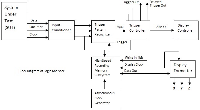
Logic Analyzer Block Diagram ~ Electronics and Communication
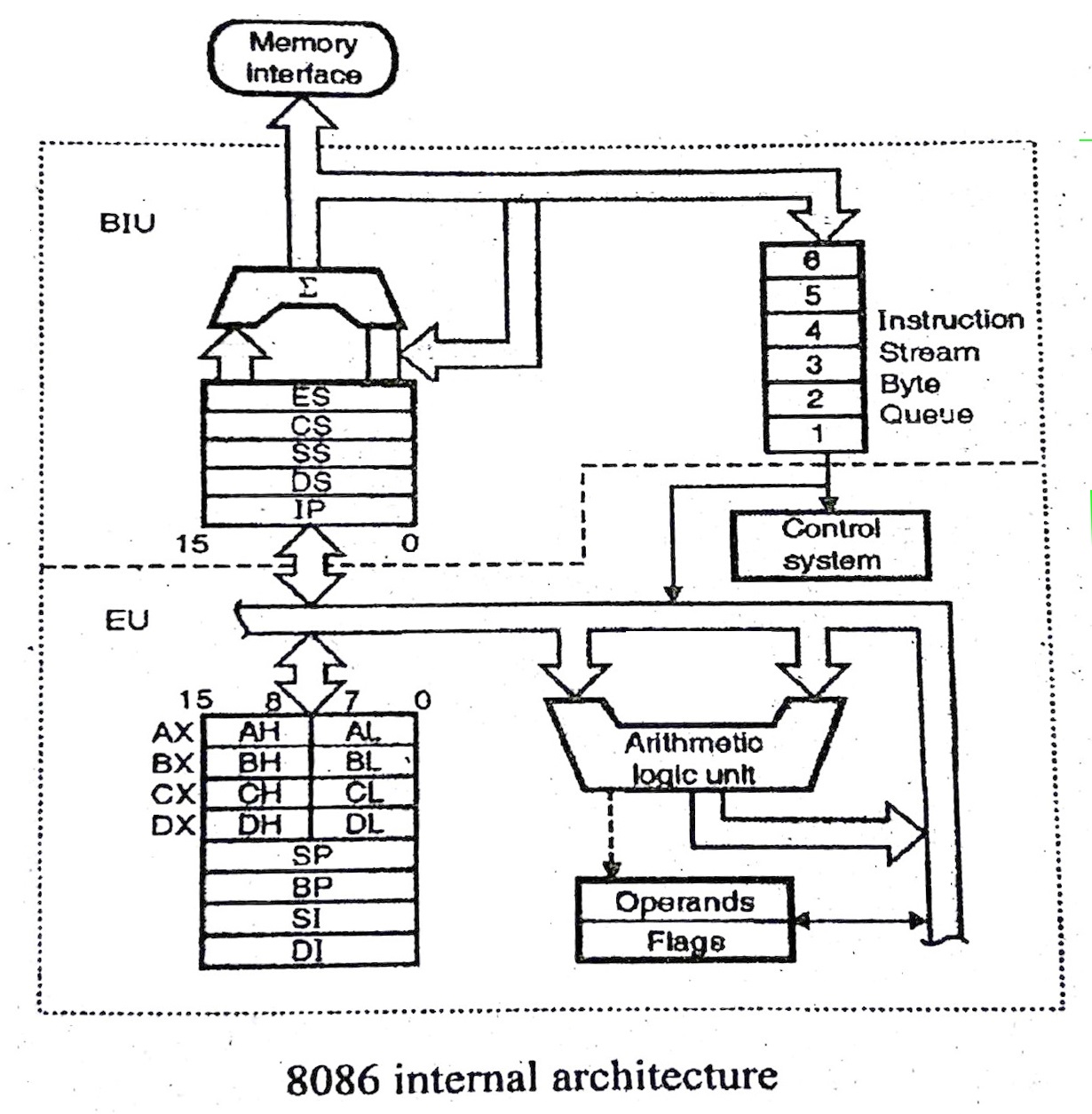
Explain the block diagram of 8086 microprocessor. - M.M.R cse
Programmable Logic Controller Block Diagram - Electronic Products

Draw logic circuit for a converter that converts 4 bit binary input to
![Experience Accelerator Logical Block Diagram [8] | Download Scientific](https://i2.wp.com/www.researchgate.net/profile/Jon-Wade/publication/307537903/figure/fig1/AS:565380533809153@1511808631242/Experience-Accelerator-Logical-Block-Diagram-8.png)
Experience Accelerator Logical Block Diagram [8] | Download Scientific